


 A surface emitting laser that produces blue light would pave the way for a number of applications, just like the blue LED has done. Several research teams have attempted to create a blue VCSEL, but have encountered problems. A research team at Chalmers has pinpointed a fundamental error in the laser design that many groups are using. This insight may be the first step towards a functioning component.
The majority surface emitting lasers – known as VCSELs (Vertical Cavity Surface Emitting Lasers) – sold today are gallium arsenide based and produce infrared light (IR).
Blue light has a shorter wavelength (between 400 and 500 nm), and many want to use gallium nitride for this. At present, GaN is used only for edge emitting lasers, which have found a home in products such as Blu-Ray DVD players.
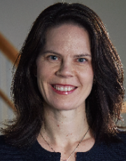 |
| Åsa Haglund |
– IR lasers exist both as edge-emitting and surface-emitting devices. We want to try to make surface-emitting GaN-based lasers, says Associate Professor Åsa Haglund, who is leading the research team.
The lasers are fabricated on wafers. An advantage of the surface-emitting variant is that it can be tested while it still sits on the disc. Edge-emitting lasers must be cleaved into individual components before they can be tested, which is difficult and expensive. VCSELs are also smaller with low current consumption, and during production you get a matrix of lasers that can be addressed individually.
|
||
|
||
|
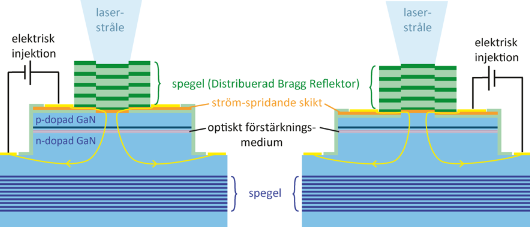
An important detail of a VCSEL is that the mirrors between which the light lases have extremely high reflectivity – well over 99 percent.
– To achieve this, you use two materials with high and low refractive index. They are alternated and stacked.
This brings the first challenge. To be able to grow different materials on each other epitaxially, they must have the same atom-atom spacing in their crystal structures. Otherwise, you add stress that causes cracks. The aluminium arsenide (AlAs) works well for GaAs-based lasers, but stacking nitrides has proven to be difficult.
The choice was made to instead build up dielectric mirrors, for example by depositing layers of silicon dioxide and titanium dioxide.
– This is what everyone has done with the upper mirror, while a few have tried to create a dielectric mirror on the bottom too. The latter is a complicated and expensive process, explains Åsa Haglund. She continues:
– I know of three companies in the world who are currently working with surface-emitting GaN lasers with dielectric mirrors. They are Sony, Panasonic and Nichia.
Nichia is well known because Shuji Nakamura worked there when he developed the first GaN-based blue LED with practical applications – a feat that awarded him and two others with the Nobel Prize in Physics in 2014.
The team at Chalmers has a different focus in their research on VCSELs in GaN.
– What sets us apart from most other university teams around the world is our very strong component focus. We have been working with surface emitting lasers in GaAs for many years. Most others are materials experts and know GaN.
– So, when we started with this, we felt that GaN lasers do not have an optimal structure. Virtually everyone has resolved issues with current injection using a design where the dielectric mirror is slightly depressed in the middle, which causes problems.
Simulations at Chalmers show that a sunken mirror produces extremely high losses (see figure 2). In many cases, the losses are so high that they cannot achieve any lasing whatsoever.
– Many have encountered this. They have not been able to get their design to lase, but they have not understood why.
Based on this discovery, the Chalmers team has developed some different design proposals where the mirror is not depressed in the middle.
– Several research groups have jumped on to what we did. They have tried to realise our proposal and have been able to present much better lasers. It makes us really happy, says Åsa Haglund. She continues:
– We hope that our research team will be able to demonstrate a good blue VCSEL within two to three years.
By ”good” she means a laser that can deliver 1 mW in optical output power at a threshold current density below 10 kA/cm2 and that has a lifetime of at least a few thousand hours.
– I think improving current injection is most important. Today, there is one team that achieved 3 mW and some that have achieved 1 mW, but the lasers burn up immediately.
At the same time, Åsa Haglund's research team is working on yet another challenge – making the lower mirror of the design electrically conductive. If this was possible, the current could go through the mirror.
Then the bottom contact, which is currently located on the side of the laser, could be positioned on the bottom of the substrate. This would avoid having to etch down the sides for the contacts. It would also make the laser thinner and smaller.
– We have managed to make nitride-based mirrors in GaN/AIN with high reflectivity and the highest electrical conductivity achieved to date. But, compared to GaAs-based VCSELs, there is still a way to go.
PHOTO: Henrik Sandsjö